

If you were actually to dismantle an electronic item and take a peek within, you are going to incredibly commonly find a platter or even a board with various elements adhered onto it– this is actually the Printed Circuit Board and also it is essentially the adhesive that hooks up all the various parts together as well as makes them function.
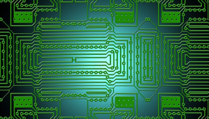
PCB means a Printed Circuit Board and is essentially a part of the board that is composed of printed cords that offer electric connection for all the elements assembled on the PCB.
The manner in which a PCB has the ability to carry out electrical energy is actually through a collection of copper wires that have been diligently put on its own area. The pattern of these cords is what ultimately establish how the product works as well as the purpose it fulfills. You can easily picture those wires to become like streets that attach various property.
Therefore despite the fact that they might look benign and also inconspicuous and not everything challenging to produce considering it’s simply a board with a couple of circuits on it, it is an important component that really goes through rather an intricate manufacturing process.
Permit’s take an overarching consider the production process that leads to the creation of a Printed Circuit Board and exactly how each measure supports its development.
PCB Manufacturing Process
Step 1: the layout
The procedure of any type of production method begins with the advancement of an essential layout. A comprehensive blueprint of the circuit board should possess been actually developed before you start.
Step 2: the print
The PCB is printed utilizing a plotted laser printer which makes a resultant film that presents the numerous coatings and details of the circuit board. The dark ink will certainly work with the conductive copper process as well as circuits while the crystal clear ink embodies the nonconductive regions. This is applicable to the inner levels. When we meet the external layers, this portrayal is reversed.
Step 3: the substrate
The substratum is composed of insulating material, particularly epoxy resin as well as glass thread. The objective of the substratum is actually to connect each one of the several components. The products are actually semi-cured in an oven and after that, the layout of the board is actually engraved onto it.
Step 4: the layers
A laminate is made of the interior levels utilizing the master plans. Treatment this laminate is a photosensitive film called the withstand which will harden under Ultraviolet lighting, assisting in the alignment as well as the printing of the circuit board in addition to boring holes.
Step 5: the bonding
The doors are actually then delivered to an area where they are revealed to beams of Ultraviolet lighting if you want to harden the photoresist level. This in fact exposes the underlying copper process and also connections.
Step 6: the refining
An alkaline chemical answer is utilized to get rid of any kind of excess copper coming from the board without inducing any sort of injury to the photoresist layer.
Step 7: the evaluation
The coatings are examined by automated devices to make sure that everything is actually lined up and in position.
Step 8: the lamination, pressing, as well as exploration
All of the coatings are actually now pressed together and laminated as they are actually held in the area along with clamps making use of an epoxy substance called prepreg. Over the prepreg is actually a coating of substratum and copper foil, topped o with more substance and also an additional copper layer. A mechanical push at that point presses whatever with each other as well as punches pins with all of them to maintain them in position. Heat energy and pressure are related to melt the epoxy and induce the layers to fuse. Last but not least, a pc assisted grill is used to bore on several gaps through the coatings, therefore, concerning reveal the substrate and also the inner panels.
Step 9: the plating
The boards are actually first extensively cleaned up and afterward are bathed in a collection of chemicals which transfers a thin coating of copper externally of the board. This coper covers the plate as well as goes into the wall structures of solitary confinements.
Step 10: the exterior level image resolution
Like one of the actions stated before, our experts administer a photoresist once again while imaging the outer levels of the layout and afterward harden it using Ultraviolet lighting. The panel at that point undergoes a machine that takes out the undesirable and also unhardened photoresist, eventually resulting in a product that is generally a contradiction of the internal layers of the PCB style.
Step 11: the plating
Using electroplating procedures, a thin level of copper is actually related to the board and the subjected locations take up the component. After that, the board undergoes container plating which protects the rooting copper paths that are indicated to create the several roads and also links of the circuit.
Step 12: the final etch
In this step, the container performs to guard the copper product that is actually called for on the board from being eliminated while the various other littles and pieces that stay subjected and also unprotected are actually removed making use of a chemical. This develops conducting places, relationships, as well as paths.
Step 13: the request of the solder face mask
This is the point where the Printed Circuit Board is ready for a coating of solder hide. It is important to make sure that the doors are actually tidy heretofore layer is applied. This is basically an epoxy solder disguise in that is later on hardened utilizing Ultraviolet lighting through a solder disguise photograph movie. This in fact gives the board its own particular environment-friendly color.
Step 14: the area finish
A surface finish is actually the last solderable coating which will definitely aid strengthen the building of the elements to the board as well as improve the top quality of the adhesion, this appearance can be attained using a number of different materials, consisting of silver and also gold.
Step 15: the silkscreen
As it nears finalization, the printed board is silkscreened making use of an inkjet which really publishes out the vital relevant information linked with the board onto it as the last coating.
Step 16: the final examination
An electrical test is operated on the freshly synthesized circuit board if you want to make sure that it remains in functioning order as well as uses the capability it is actually expected to. This might either be carried out through a practiced professional or in an automatic fashion in a controlled environment. The testing design depends on the original concepts of the board.
Step 17: the cutting
Once the developing, completion and screening is total, the manufacturing of the PCB is actually delivered to a shut through an equipment reducing out a number of boards coming from an authentic board utilizing a modem or even a v gouge, along with the previous leave of absence tabs on the edges of the reduced outboard for extraction as well as the last cutting diagonal networks on either sides of the board